Newly Upgraded Nanotechnology Labs Advance Science, Learning
In the Stanford Nanocharacterization Lab, Mechanical Engineering Professor Xiaolin Zheng, is studying nanowires “decorated” with tiny particles in a way that could lead to better batteries, solar cells and catalysts.
Kathryn Moler, a professor in the departments of applied physics and physics, and Brian Rutt, PhD, professor of radiology, are working in the Stanford Nano Center to genetically engineer mammalian cells to express magnetic particles. If they succeed, it may be possible to use MRIs to track individual cancer cells and stem cells as they move through the body.
And in the Stanford Nanofabrication Facility, a team led by Electrical Engineering Professor Jelena Vuckovic is developing nanoscale light-based devices that transmit data at ultrafast rates while using thousands of times less energy than current technologies. The work could one day help speed up computers and dramatically reduce power consumption.
Fresh off a multimillion-dollar upgrade and equipped with new, more sophisticated instruments, Stanford’s three largest shared nanotechnology facilities now rank among the best in the world. Located in or near the Science and Engineering Quad, the labs give researchers both inside and outside Stanford access to trained staff and equipment that would be too costly for any single researcher to acquire.
“Shared facilities that offer access to state-of-the-art scientific instruments are an essential resource for Stanford’s faculty and students,” said Ann Arvin, Vice Provost and Dean of Research. “Having these remarkable research tools and highly skilled research scientists to guide their use is certain to create scientific advances and insights that we cannot begin to predict.”

Research scientist Ai Leen Koh works at the FEI Titan TEM (transmission electron microscope) in the Stanford Nano Center. Photo: Joel Simon
Advancing Nanotechnology
“The efforts made campus-wide to renew the nano facilities have been tremendous. We can do research we couldn’t do without the shared equipment,” said Moler, who is also faculty director of the 9,000-square-foot Stanford Nano Center (SNC), which became the newest shared nano facility when it opened in March 2011.
Nanotechnology is considered one of the most promising areas for scientific discovery. Already nanotechnology is helping improve and in some cases revolutionize IT, energy, environmental science, medicine, homeland security, food safety and transportation – enabling faster and more portable computers, less flammable and more efficient batteries, earlier diagnosis of some diseases, tougher machine parts and much more.
In the future, researchers expect the ability to create materials and devices at the scale of one-billionth of a meter could bring about more affordable and efficient clean energy, novel computing systems, radical new approaches to disease diagnosis and treatment, and much more.
“The applications for nanotechnology -- in medicine and biotechnology, information technology and energy -- are hugely important for society across the board,” said Roger Howe, the William E. Ayer Professor of Engineering and the faculty director for the Stanford Nanofabrication Facility (SNF).
Landmark Discoveries
The shared facilities together operate as a network for research and education for Stanford faculty and students, as well as a resource for researchers from other universities, government and in some cases, startups and large companies.
The facilities have already been home to some landmark discoveries. The SNF is the oldest of the three, opening in its current form in 1984 with ongoing support from the National Science Foundation. The lab and its predecessors have been home to such pioneering work as creation of what is seen as the first MEMS device, the first MIPS chip and the Atomic Force Microscope, one of the foremost tools for imaging, measuring, and manipulating matter at the nanoscale.
More recently, work conducted in the shared nano facilities has led to prototypes of a widely used DNA sequencer, a new generation of high-energy particle physics detector and advances in everything from solar cell technology to treatments for brain tumors to improved organic transistors. In one of the most exciting developments researchers have pushed the field of plasmonics into a new realm that could have lasting consequences for catalytic processes such as artificial photosynthesis, for cancer research and treatment, and even quantum computing.

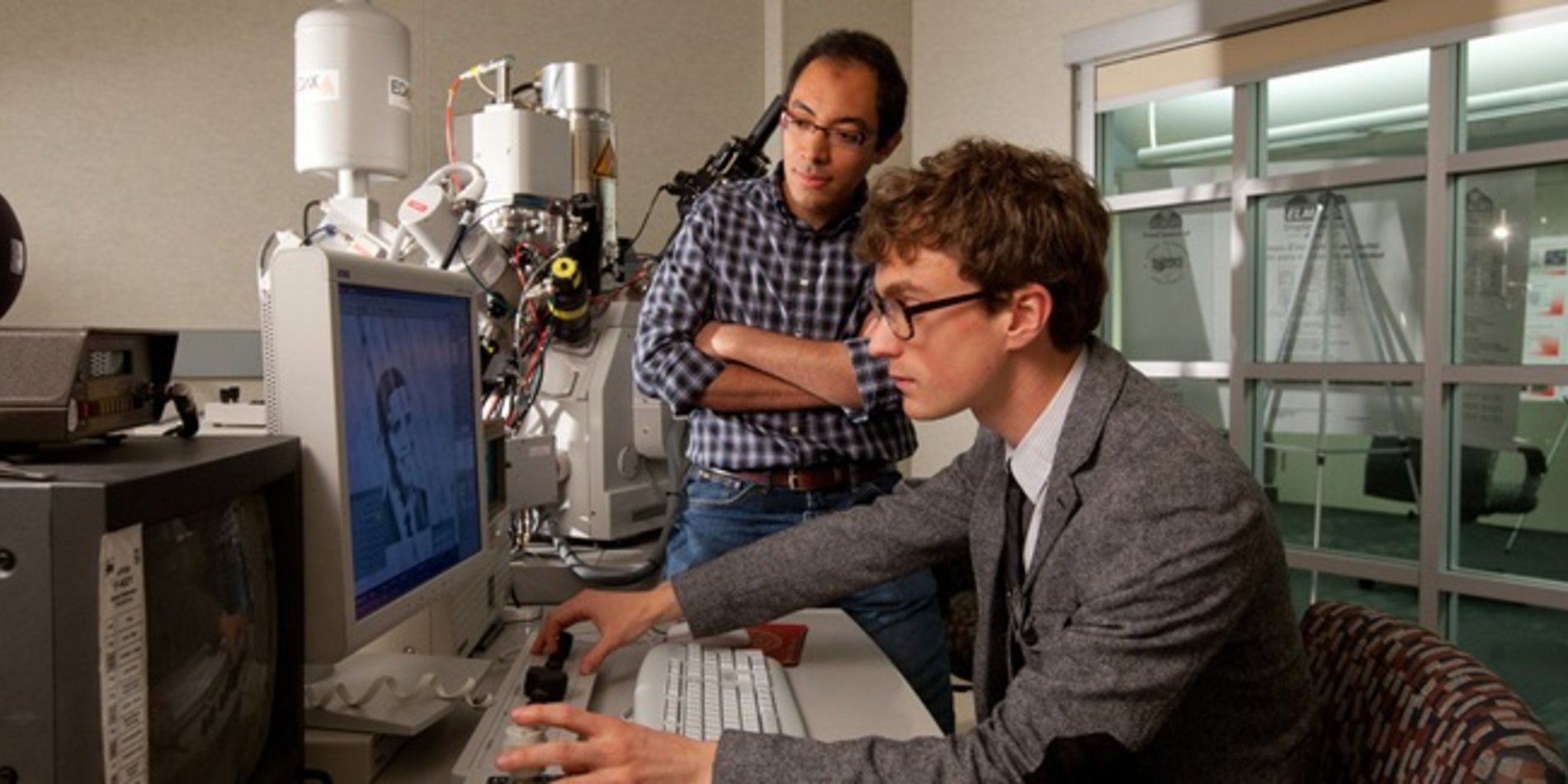
MSE grad student Brian Baum (seated) and EE PhD student Amr Saleh (standing) in the Focused Ion Beam (FIB) Lab, part of the Stanford Nanocharacterization Laboratory. Photo: Joel Simon
“The investment by the university in the shared facilities in the Stanford Nanocharacterization Lab has had a huge impact on the scientific level of the research that is being carried out,” said Robert Sinclair, chairman of the Materials Science and Engineering Department and director of the lab. “It has raised the quality of the work we are doing to the forefront of international research.”
More Labs Planned
With the expected completion of Stanford’s Biological and Chemical Engineering Building in 2014, the university is planning to open more shared research facilities with new capabilities for imaging living cells and tissue; producing and characterizing proteins and small molecules, and optogenetics, a research technique that allows researchers to fashion mammalian tissues that are responsive to light.
In addition to enabling research that could not be conducted otherwise, shared facilities “provide tremendous opportunities for cross-fertilization – of people, ideas and disciplines,” said Curt Frank, senior associate dean for faculty affairs in the School of Engineering. “That’s a very strong benefit.”
Jamie Beckett is director of communications and alumni relations for the Stanford University School of Engineering.


